
In the ever-evolving landscape of technology, one trend that continues to gain momentum is the growing demand for compact devices. As the world moves toward smaller, more efficient electronics, manufacturers and designers are constantly looking for ways to integrate advanced features without compromising on size or performance. One technology that has played a crucial role in this shift is HDI PCBs (High-Density Interconnect Printed Circuit Boards). These innovative boards have become the backbone of modern electronics, enabling the development of ultra-compact devices with enhanced functionality.
What is an HDI PCB?
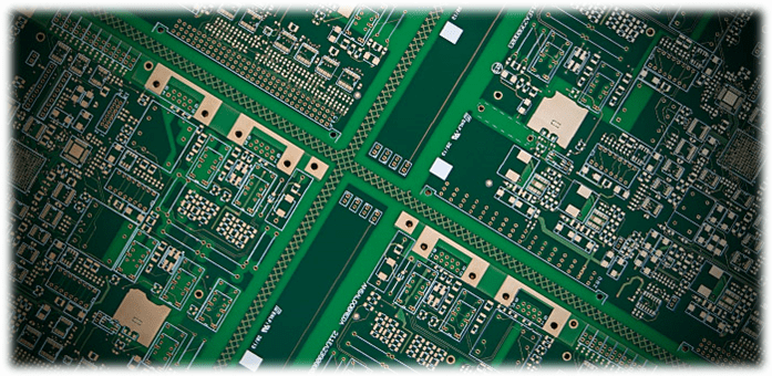
HDI PCBs are advanced circuit boards characterized by their high component density, which allows for the creation of smaller and more efficient electronic devices. They use finer traces and smaller vias, which means more components can fit into a smaller space. This technology is essential for the production of compact devices, from smartphones to medical equipment, as it allows for the integration of more features in less space without sacrificing performance.
HDI PCBs are different from traditional PCBs because they incorporate advanced manufacturing techniques, such as microvias, blind and buried vias, and fine-pitch components. These techniques enable the production of more complex circuit boards that support the increasingly high-performance requirements of today’s electronic devices.
The Role of HDI PCBs in Compact Devices
Compact devices are becoming an integral part of everyday life. From the smartphones we carry in our pockets to the wearable fitness trackers we use, the demand for smaller devices with more features has skyrocketed. This demand is only possible thanks to the advancements in HDI PCBs. Here’s how HDI PCBs are shaping the future of compact devices:
Enhanced Functionality in Smaller Packages
One of the main advantages of HDI PCBs is their ability to pack more components into a smaller area. Traditional PCBs require larger spaces for components like resistors, capacitors, and chips. With HDI PCBs, manufacturers can use smaller components and more complex layouts, allowing for more functionality in a compact design. As a result, devices like smartphones, tablets, and wearables can offer more advanced features without increasing in size.
Better Performance
In compact devices, performance is often a key concern. The smaller the device, the harder it becomes to ensure efficient heat dissipation, signal integrity, and power consumption. HDI PCBs offer several advantages in this regard. Due to their smaller vias and traces, HDI PCBs have improved signal integrity and can handle higher frequencies. Additionally, the precise design allows for more effective heat dissipation, ensuring that devices remain cool even under heavy use. This makes them an ideal choice for applications that require high-speed data transmission and processing, such as 5G devices, drones, and advanced wearables.
Cost Efficiency
While HDI PCBs offer exceptional performance and miniaturization, they also help reduce the overall cost of production. By using fewer materials and enabling more efficient designs, manufacturers can reduce material costs, assembly time, and waste. Additionally, the ability to fit more functionality into smaller devices can make the production of these devices more cost-effective in the long run.
Reliability and Durability
Compact devices need to be both reliable and durable. Whether it’s a smartphone subjected to drops and impacts or a medical device used in extreme conditions, HDI PCBs are built to withstand harsh environments. The advanced construction methods used in HDI PCB manufacturing provide enhanced strength and resilience. These boards can tolerate higher temperatures, vibrations, and physical stresses, ensuring that the device functions reliably over its lifetime.
Innovation in Consumer Electronics
As consumer electronics become more advanced, there’s an increasing need for compact designs that don’t sacrifice performance. HDI PCBs have enabled groundbreaking innovations in devices such as foldable smartphones, augmented reality (AR) glasses, and miniature drones. The smaller form factor of these devices is made possible by the use of HDI PCBs, which allow for a dense and compact arrangement of electronic components while maintaining signal integrity and performance.
Key Industries Benefiting from HDI PCBs
While HDI PCBs are essential for consumer electronics, several industries are set to benefit from this technology as well. Here are a few industries where HDI PCBs are playing a significant role:
- Medical Devices: Compact, portable, and highly reliable medical devices are critical in healthcare. HDI PCBs enable the development of smaller, more efficient medical devices like pacemakers, insulin pumps, and diagnostic equipment, offering improved functionality and precision.
- Automotive: With the rise of autonomous vehicles and electric vehicles (EVs), HDI PCBs are becoming crucial for integrating advanced sensors, navigation systems, and power management features in small, efficient designs. These boards ensure that the electronics in vehicles can operate reliably under harsh conditions.
- Internet of Things (IoT): IoT devices, including smart home gadgets, wearables, and sensors, require small form factors and high performance. HDI PCBs are the ideal solution, enabling the miniaturization of these devices while enhancing connectivity and functionality.
- Aerospace and Defense: HDI PCBs are also used in high-performance systems found in aerospace and defense technologies, where reliability, compactness, and performance are critical. From communication systems to navigation and control equipment, HDI PCBs ensure that these systems operate efficiently in extreme environments.
The Future Outlook for HDI PCBs
Looking ahead, HDI PCBs will continue to evolve, pushing the boundaries of miniaturization and performance. As consumer demands for even more compact and feature-rich devices grow, manufacturers will rely on these advanced circuit boards to meet those expectations. The future of HDI PCBs will be shaped by innovations in materials, manufacturing processes, and design techniques that enable even smaller, faster, and more powerful devices.
Additionally, as emerging technologies like 5G, artificial intelligence (AI), and the Internet of Things continue to expand, HDI PCBs will play a critical role in supporting the complex, high-speed circuits required by these technologies. For those looking to explore more about HDI PCBs and their applications, check over here for detailed resources and insights.
Conclusion
The future of compact devices lies in the hands of innovative technologies, and HDI PCBs are at the forefront of this revolution. By enabling smaller, more efficient, and high-performing devices, these circuit boards have paved the way for the next generation of electronics. Whether in smartphones, medical devices, or automotive applications, HDI PCBs are shaping the devices we use every day.
In conclusion, HDI PCBs are not just an advancement in circuit board technology; they are the key to unlocking the future of compact devices that continue to evolve, becoming more powerful, efficient, and multifunctional in ways we never thought possible.